Login to your Account
Design
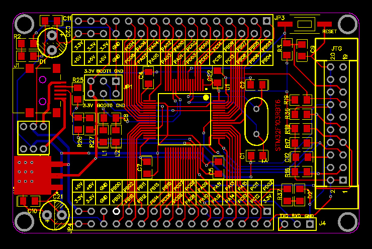
PCB Design
Printed circuit board (PCB) layout and design services is one of the ways that we help our customers get to market faster as our engineering team has significant real world experience designing PCBs for performance and manufacturability.
PCB
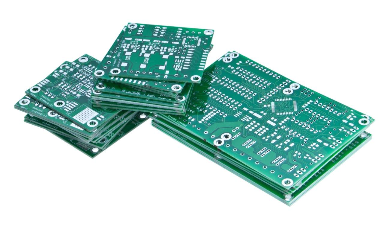
Printed Circuit Board Fabrication
Single Side, double Side and Multilayer Layer PCB's
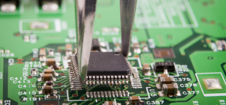
Assembling
PCB Assembling
A few preparatory steps have to happen before real PCBA process even begins. This helps PCB manufacturers assess the functionality of a PCB design, and includes of QC check.
Type of PCB Materials
FR2, FR4(Glass of Epoxy)
PCB Thickness Available
0.8mm, 1mm, 1.2mm, 1.6mm, 2.4mm, 3.2mm
( Copper OZ : 1 and 2 )
Lead Time
6 Day's For single layer,
8 Day's for double layer,
15 Day's for multilayer
PCB Assembling
Manual Soldering, Automatic Dip Soldering, Re-flow Oven, Wave Soldering
Packages
QFN, QFP, BGA